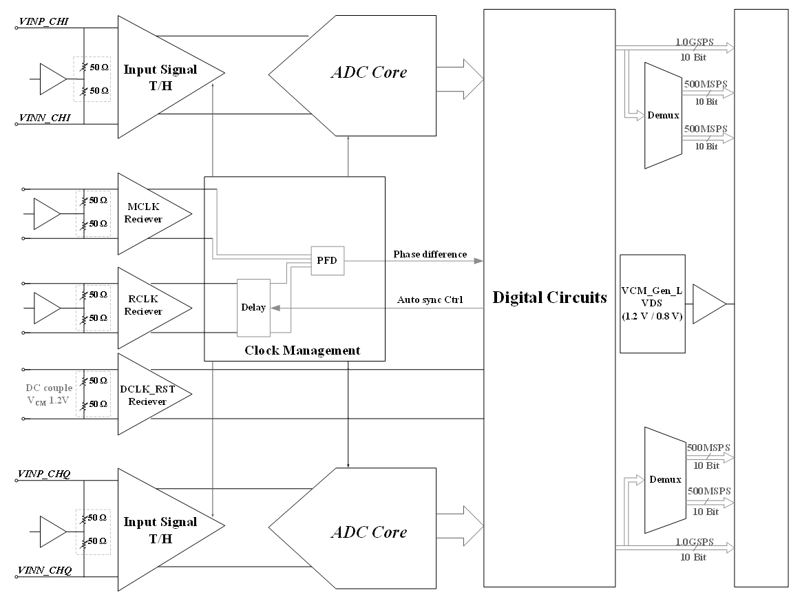
Functional Block Diagram
Product Highlights:
- Package and pinout fully compatible with the reference model ADC10D1000, enabling seamless pin-to-pin replacement.
- Optimized for low power consumption—approximately 56% of the reference device, eliminating the need for a heatsink.
- 25% shorter conversion latency compared to the reference device, improving overall system responsiveness.
- Wider operating temperature range, offering better environmental adaptability.
- Supports multi-chip AutoSync synchronization; dedicated acquisition IP available for streamlined system integration.
Key Features:
-
- Full-Power Bandwidth: 2.4 GHz
- Conversion Latency: 26 master clock cycles
- Static Performance:
— DNL: –0.8 LSB to+1.2LSB
—INL: –2.5 LSB to +2.8 LSB
- Dynamic Performance (fs = 1.0 GSPS, input signal = –1 dBFS):
—fin=100MHz
- ENOB=8.2Bit
- SFDR=64.7dBFS
- SNR=51.4dBFS
—fin = 248MHz
- ENOB=8.1Bit
- SFDR=62.6dBFS
- SNR=50.9dBFS
—fin = 498MHz
- ENOB=7.9Bit
- SFDR=63.3dBFS
- SNR=49.9dBFS
—fin = 750MHz
- ENOB=7.7Bit
- SFDR=63.9dBFS
- SNR=48.4dBFS
Applications:
-
- Wideband communications
- Data acquisition systems
- Digital oscilloscopes