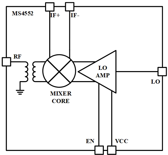
The MS4552 is a wideband RF mixer designed for operation from 3 GHz to 20 GHz. It features a differential IF port, which can be converted to single-ended using an external balun depending on the IF frequency. The differential interface is particularly suitable for low-IF applications below 500 MHz, and can be directly connected to differential filters or IF amplifiers.
The device supports:
RF frequency range: 3~20 GHz
LO frequency range: 1~20 GHz
IF frequency range: DC~6 GHz
All ports exhibit ultra-wideband characteristics. The chip integrates an on-chip LO amplifier, enabling operation with a typical LO drive of 0 dBm, without requiring external gain stages.
Powered by a single 3.3 V supply, the MS4552 offers a simple and user-friendly design.
The device is available in a QFN package (MS4552E) and bare die form (MS4552K), supports an operating temperature range of –40°C to +125°C, and delivers outstanding wideband performance.
It is suitable for use in microwave transceivers, wireless backhaul, point-to-point communication, phased array antennas, C/X/Ku-band radar systems, test equipment, and satellite modem systems.