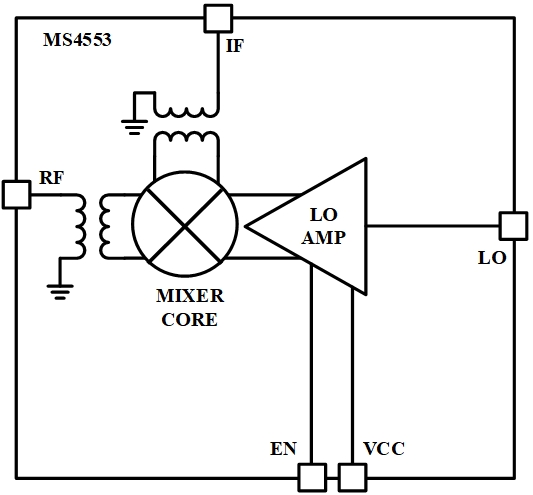
The MS4553 is a wideband RF mixer operating from 3 GHz to 20 GHz. It features an integrated on-chip balun on the IF port, providing a single-ended interface for simplified cascading with subsequent circuits.
The device supports:
RF input range: 3–20 GHz
LO input range: 1–20 GHz
IF output range: 0.5–9 GHz
All ports deliver ultra-wideband performance. An integrated LO amplifier enables operation with a typical LO drive of 0 dBm, simplifying the LO drive requirements.
The MS4553 operates from a single 3.3 V power supply, making it easy to use and ideal for space- and power-constrained systems.
It is available in both a QFN package (MS4553E) and bare die form (MS4553K), supports an operating temperature range of –40°C to +125°C, and delivers excellent RF performance across its full frequency range.
The MS4553 is ideal for use in microwave transceivers, wireless backhaul, point-to-point communication, phased array antennas, C/X/Ku-band radar systems, test instrumentation, and satellite modem applications.